Services
Turnkey Solutions
USEA provides turnkey solutions for semiconductor devices and components from wafer sort through assembly, parametric testing, and final functional testing Hot, Cold, and Ambient. Customer view their work in progress (WIP) on our cloud-based WIP. Our turnkey solutions allow a seamless scale-up option from a few parts to millions of parts per month.
Advanced Statistical Analysis – The DataCruncher™ can process large amounts of data to analyze correlation, statistical significance of process change, and failure analysis.
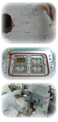
Failure Analysis Capabilities – We go beyond traditional Failure Analysis methods, offering a comprehensive suite of advanced tools and expert engineering to discover the root causes of complex failures. Our technology allows us to examine deep into the details of products failures.
Failure Analysis Capabilities:
- Identify wire-related defects with precision.
- Measure die-attached voids for detailed internal assessments.
- Detect internal cracks and interfacial delamination in non-hermetic products, ensuring structural integrity.
- Perform cross-sectional analysis to examine internal planes destructively, revealing hidden flaws.
- Verify unit current/voltage characteristics, ensuring components meet standards.
- Conduct visual inspections at both high and low magnifications to uncover defects and anomalies not visible to the naked eye.
- Remove encapsulating materials to expose internal parts, enabling thorough visual inspections.
- Pinpoint abnormal heat locations at the die level, crucial for identifying leakage failures.
- Evaluate die-level current/voltage characteristics with high precision, using a curve tracer for accuracy.
- Ensure reliability with Solderability and Resistance to Solder Heat tests, critical for long-term performance.
- Utilize Pressure Cooker Test Chambers, Temperature Cycle Tests, and High-Temperature Storage Life Tests to simulate and analyze real-world environmental conditions.
- Classify moisture sensitivity levels and assess reflow profiles, safeguarding your products from moisture-induced failures.
- Conduct Lead Fatigue Tests and Unbiased Temperature and Humidity Tests to ensure your products can withstand the rigors of operational environments
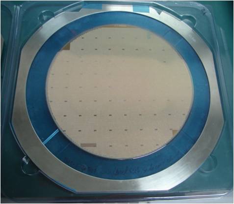
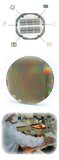
Wafers Test (Sort)
High throughput wafer sort bumped or bare die after or before saw.
Wafer mapping and sorting services:
- Testing After Saw – Proprietary technology for highly parallel probing of wafers after saw at multiple temperatures (-55°C to 200°C).
- Unique Specialty Testing – High throughput specialty testing including UIL/UIS (Avalanche), RG/CG, QG, and DC testing through our QM1000 tester.
- Test Data in Real Time – Test data are uploaded in real time to the cloud to enable our customers to monitor their test data in real time through our Datacruncher™ tool.
- WIP Tracking – Online tracking of work orders through the WIP tool.
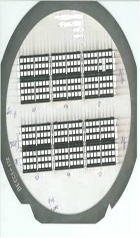
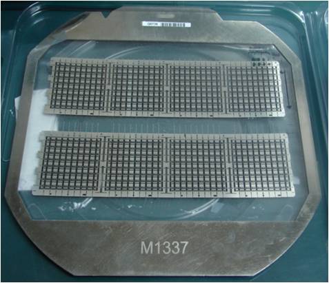
Chip Scale Package
Testing on Film Frame
USEA has developed proprietary technology for the highly parallel testing of parts after saw. Our technology fixes the die in position after the saw processes, with minimal x-y displacement. This allows for highly parallel testing of the die at temperatures ranging from -55°C to 200°C on automated test equipment.
Benefits our customers and collaborators both during their engineering and production phases by:
- Increased Throughput (UPH) – Testing at high volume, our technology increases the test yield for chip scale, bumped die, and singulated die on the film frame handler and or prober. The result is elimination of jams associated with turret and gravity feed handlers and increasing test yield.
- Reduced Tooling Costs – The tooling costs for handling chip scale packages on handlers such as turret and gravity feed handlers are avoided when handling the parts on the film frame handler.
- Reduced Engineering Setup Time – The engineering time required to implement a change kit on turret and gravity feed handlers is eliminated.
- Tri-Temperature Testing – Film frame handlers strategy supports testing of parts at multiple temperatures ranging from -40°C to 85°C.
- Test After Saw – Mechanical and chemical damage to device functionality from the saw process are test rejects when testing after saw.
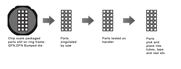
Traditional Strategy
The traditional approach for handling CSP involves singulation the devices on the film frame, then separating them from it. The issue with this method is that while the devices remain highly ordered and easy to handle and test before singulation, once separated from the film frame they become disordered. This requires additional effort to re-order them and verify their orientation for testing and packaging (see figure below).
100% of the production and characterization test data are available for analysis with the cloud-based DataCruncher™.
Testing After Saw
USEA has developed proprietary technology for the highly parallel testing of parts after saw. Our technology fixes the die in position after the saw processes, with minimal x-y displacement. This allows for highly parallel testing of the die at temperatures ranging from -55°C to 200°C on automated test equipment.
Benefits our customers and collaborators during their engineering and production phases by:
- Placement of Components – Next to probe technology is the only solution for placing discrete components directly next to the device under test for devices. The strategy allows for testing otherwise not possible and for increasing test yield.
- Increased Throughput (UPH) – When testing at high volume, USEA’s technology dramatically increases the test speed for chip scale, bumped die, and singulated die on the film frame handler. This is achieved through elimination of jams associated with turret and gravity feed handlers, reduced indexing time between tests, and reduced engineer supervision requirements.
- Reduced Tooling Costs – The tooling costs for handling chip scale packages on handlers such as turret and gravity feed handlers are avoided when handling the parts on the film frame handler.
- Reduced Engineering Setup Costs – The engineering time required to implement a change kit on turret and gravity feed handlers is eliminated and replaced with a lower effort alignment procedure on the film frame handler.
- Tri-Temperature Testing – USEA’s film frame handler strategy allows for the testing of parts at multiple temperatures ranging from -40°C to 85°C.
- Reduced Test Costs – The increased throughput of testing coupled with lower engineering setup costs and associated NRE results in a lower test cost and higher customer margins.
- Test After Saw – The mechanical and chemical damage to parts that sometimes occurs during the saw process is screened for using the testing after saw technology.
Specialty Testing
USEA has developed test solutions that allow highly parallel specialty testing (including UIL/UIS, RG/CG, QG, and DC) of wafers and packaged die on single insertions. The QM1000™ quad-site tester offers up to a 4X increase in throughput.
Low cost, high throughput testing service and projects from USEA.
Ideal for specialty testing of:
- MOSFETs
- SiC-Type (Silicon Carbide) Semiconductors
- GaN-Type (Gallium Nitride) Semiconductors
- JFETs
- FETs
- IGBTs
- BJTs
- Diodes
- Mixed Signal ICs
- Discrete Analog Devices
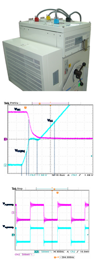
Tri-Temperature Testing
USEA routinely runs production testing and engineering scale characterization programs at temperatures from -55 °C to 150 °C. Routine production testing temperatures include:
–55 °C
–40 °C
0 °C
Room Temperature
80 °C
120 °C
150 °C
USEA collects 100% of the production and characterization test data which are available for examination through our proprietary cloud-based database DataCruncher™. During an engineering characterization program, USEA is able to translate all of the test data into graphs and datasheets ready for our clients’ engineering, production, and marketing groups.
USEA has a wide range of equipment optimized for performing tests at these temperatures.
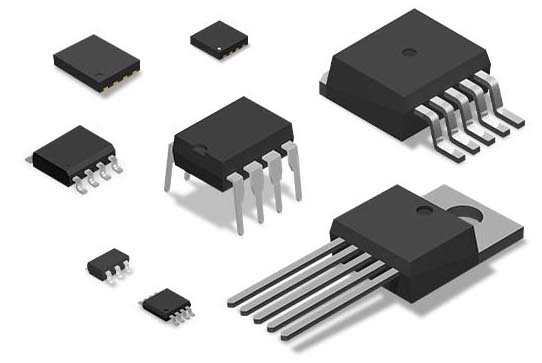
Products Tested
We have experienced in production-scale testing of analog and mixed signal devices and in new wide band gap materials including GaN and SiC semiconductors. Devices that have been tested at USEA includes:
• Automotive Applications
• Aircraft & Space Applications
• Seacraft Applications
• Robotics & Drones
• Renewable Energy
• Wireless Communications
• Temperature Sensors
• Power & Battery Management Devices
• MOSFETs & IGBTs
• Analog Switches
• Temperature Sensors
• Motor Controllers
• Precision Voltage References
• Telecom Devices
• Op-Amps & Regulators
• USB Port Controllers
• Mixed Signal Devices
• Digital Devices
• 8 to 6 GHz Saw Filters
• HVIC & MOSFET/IGBT Driver
Work In Progress (WIP) Technology
Customers can monitor their real time WIP (Work in Progress) on the cloud.
Test Development
USEA is involved at all levels of test development, including the necessary test board design and layout, software development, socket design and build. We work on programs at all stages of the product development timeline and through to manufacturing. Examples of our test development contributions include:
- Engineering Characterization – Smaller scale engineering studies with comprehensive parametric and functional testing, including our unique multi-temperature test technologies.
- Package Qualification – This includes parametric testing, functional testing, highly-accelerated aging, and highly accelerated lifetime testing.
- Production Testing – Optimized test procedure along with parts handling strategy, including our unique test solutions.
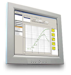
DataCruncher™
The DataCruncher™ is a comprehensive suite of device and wafer data acquisition tools designed for engineers and in-house manufacturing teams. As a web-based platform, it provides easy access to production and engineering data, from wafer sorting to final testing. The tool facilitates the creation of detailed histograms and other visual reports, helping you and your customers monitor and enhance overall device performance.
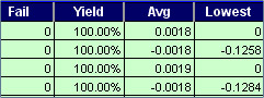
Test Data Analysis
DataCruncher™ features the most commonly used statistical calculations (Average, Standard Deviation and CPK) and presented in a report for easy analysis. Statistical Data from more than one lot can be shown side by side for easy comparison.
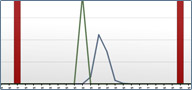
Histogram Chart
Histogram of test parameters can be produced to show trends in parametric test results. Data from multiple lots can be combined and analyzed in one chart.
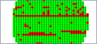
Wafer Map and Die Info
Shows a graphical map of binning test results, color coded with the bin number indicated for easy identification. Clicking on a die will show XY coordinates and bin value.
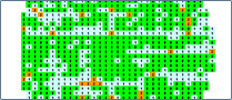
Stacked Wafer maps
Applicable to wafer probe data for showing a graphical map of binning results for a number of wafers. Tally of failed bins per wafer die position is displayed on screen.
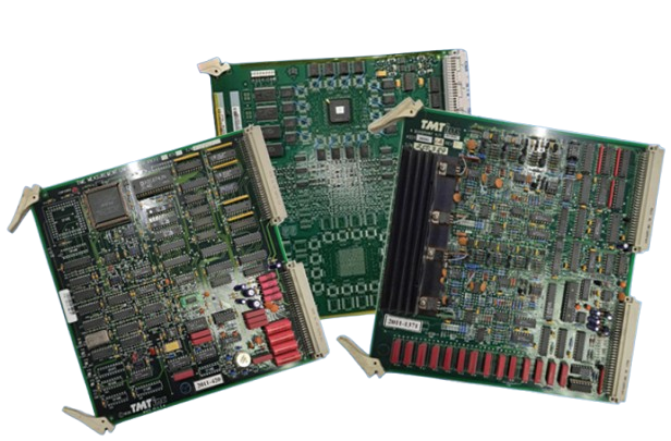
Board Repair Services
USEA engineers are experts in the repair and upgrade of ASL LTX-Credence resource boards.
Examples of boards and services we have offered in the past includes, but are not limited to:
- DVI, OVI, MUX, OAL
- TMU, DDD, ACS
- HVS, OFS, DCC
- PVI, PV2, PV3
- DOS and NT Interface Card
- Upgrade of DVI-200mA to DVI-300mA
- Upgrade of OVI-20mA to OVI-30mA
- Upgrade of HVS-650V to HVS-850V
- Respin
- Reverse Engineering
- Schematic Generation
- Board Layout
- Board Stuffing
- Board Debug
QM1000™ Quad-Site Tester
USEA recently introduced the QM1000™ quad-site instrument for testing analog and mixed signal semiconductor devices. This low cost, high throughput service and product is ideal for specialty testing of MOSFETs, SiC and GaN Semiconductors, JFETs, FETs, IGBTs, BJTs, Diodes, Mixed Signal ICs, and Discrete Analog Devices.
Designed to mate with and expand the capabilities of the LTX-Credence ASL1000, the QM1000™ performs both DC and specialty AC tests, including QG, RG/CG, and UIL/UIS (Avalanche). The ability to perform quad-site testing on a single insertion basis reduces device handling requirements and eliminates the need for multiple external instruments to fully characterize semiconductor devices. The QM1000™ offers up to 4X improvement in test throughput and yield, and is compatible with film frame, rotary, and auto handlers.
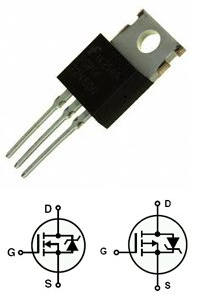
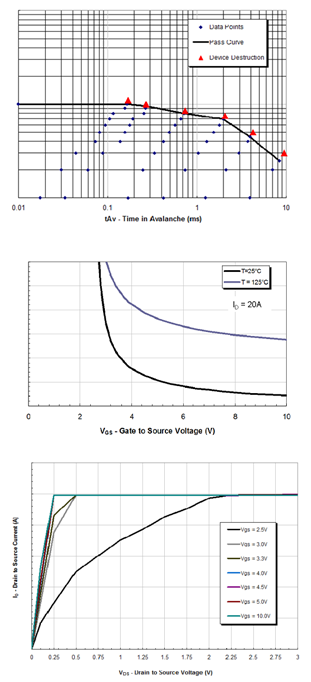
MOSFET Characterization
USEA provides MOSFET characterization services for engineering, production and marketing efforts.
The deliverable from our characterization program includes:
• Raw data
• Graphed data
• Final comprehensive report
USEA ensures data quality by verifying it against the customer’s product specification sheet and confirming internal consistency. For example, RDSON vs. VGS is checked against the typical characterization output, and Ciss is verified to align with expected Qg values, among other parameters.
USEA’s MOSFET characterization services includes:
• Output Characteristic
• Transfer Characteristics
• RDSON vs. VGS
• RDSON vs. Temperature
• Gate to Source Threshold Voltage (VGSTH) vs. Temperature
• Source to Drain Current (ISD) vs. Source to Drain Voltage (VSD)
• Drain to Source Breakdown Voltage (BVDSS) vs. Temperature
• Capacitance (Ciss, Crss and Coss) vs. Source Voltage
• Gate Charge (Qg)
USEA has over twenty years of MOSFET production and characterization testing.
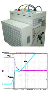
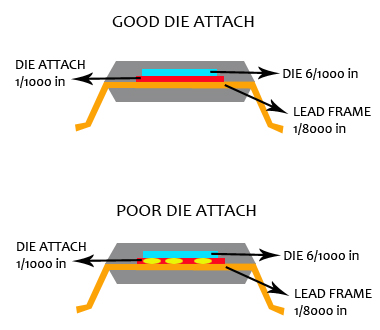
Delta VSD Engineering and Production Testing (MIL-STD-750D method 3161)
USEA understands the importance of good die attach in devices including power MOSFETs; therefore USEA develops Delta VSD (DVSD) testing for the engineering and production phases in accordance with MIL-STD-750D method 3161.
USEA provides the necessary inputs into the test development including:
• Thermal characterization of the part with regard to VSD vs. Temperature
• Test development for the initial and final VSD determination
• Test development of the appropriate heating current pulse
• Test development of the duration of the heating pulse to ensure that the test interrogates the die to lead frame attachment
• Scale engineering Delta VSD (DVSD) and perform true quadsite testing in production (link to the QM1000™ Tester)
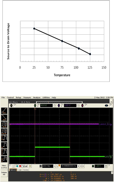
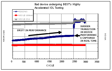
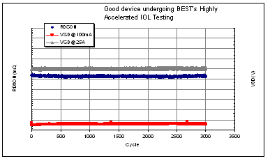
Highly Accelerated IOL
USEA’s Highly Accelerated Intermittent Operating Life (IOL) methodology is directly equivalent to MIL-STD-750 method 1037 and has multiple benefits to the engineer including:
• Continuous Measurement– The advantage is that rather than waiting for read points on the device for example at 500 temperature cycles, 1500, 7500 15,000 temperature/power cycles, the data is continuously gathered and so devices that are damaged by the cycling are seen much earlier. USEA has seen apparently “good” arts fail in as little as 200 temperature/power cycles. The implication to our customers is they have an accelerated warning that a lot is going to fail the IOL study.
• Provides Underlying Root Cause – The fact that USEA temperature cycles the devices and continuous tracks parameters such as VSD, RDSON, Vth, BVDSS, any MOSFET parameters, any IGBT parameter, diode related parameters, means that the trends in drift can be analyzed and provide additional insight into whether failure issues are related to specific parts of a device, e.g. drain, source or gate and whether failure a gradual process through migration of metal or a sudden failure due to bond failures.
• IOL Data- USEA’s highly accelerated and continuous data collection IOL studies includes full data analysis and concise report representation. The reduction of the IOL study duration from weeks to days in achieve throught:
Continuous Data Tracking- USEA is continuously monitoring the electrical and thermal parameters of all the devices throughout the study and so if devices are showing significant changes during the study then USEA is able to call this very early in the study and a warning call can go to a customer within hours of starting the test.
Optimized Thermal Tracking – USEA is able to track the temperature of individual parts during the study and so USEA is able to accelerate the thermal cycling time between heating and cooling by individually tracking the parts, rather than waiting some arbitrarily long cool down time of two or three minutes. Knowing the exact temperature of each individual device throughout the study provides optimized temperature cycling and guarantees that each device was cycled at and between the required temperature.
Tested and Cycled in Place – USEA is continuously tracking the performance of each device through out the IOL study, as we are testing and cycling the device in the same fixture. Therefore USEA has eliminated handling errors when devices are manually transitioned between cycling stations and test stations.
• Equivalence between Highly accelerated IOL vs. Traditional IOL- USEA has correlated the failures seen in traditional IOL studies with their Highly accelerated IOL studies and demonstrated that the failure mechanism is the same. This equivalence between USEA’s highly accelerated IOL studies with the traditional IOL studies come from two facts:
Same Active Heating – In both the USEA highly accelerated IOL and the traditional IOL, the source of heating comes from electrical power applied through the die, and so both tests are fundamentally identical.
Same Temperature Cycling – In both the USEA highly accelerated IOL and the traditional IOL, the devices under test are expected to temperature cycle from 25 °C to 125 °C. The advantage of the USEA highly accelerated IOL testing is that the exact temperature of the devices at any point with the IOL cycling is known and can be used in the understanding failures, outliers and maverick.